

STORY
More Stories
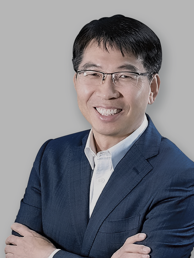
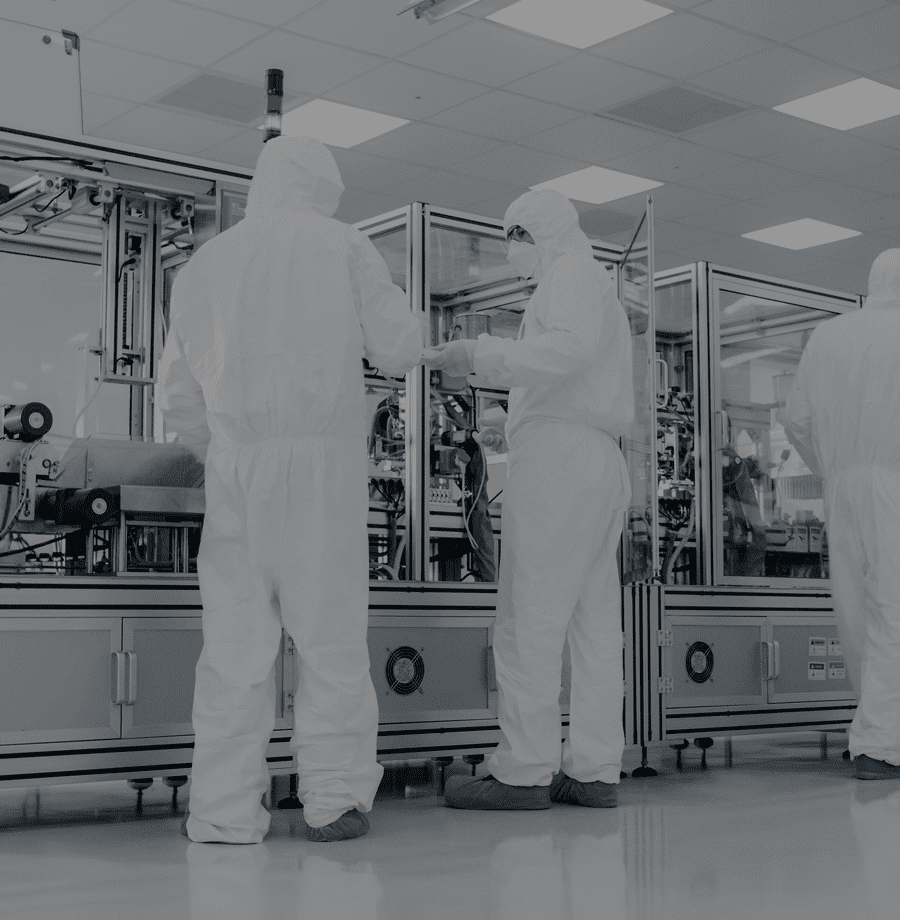
SEMES is leaping forward to emerge as a world-renowned
equipment maker
through supplying advanced
technology, extensively investing in facilities,
and
expanding its business overseas.
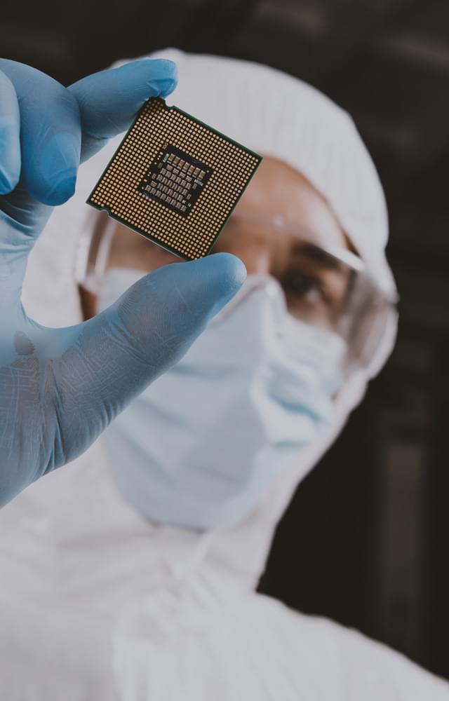
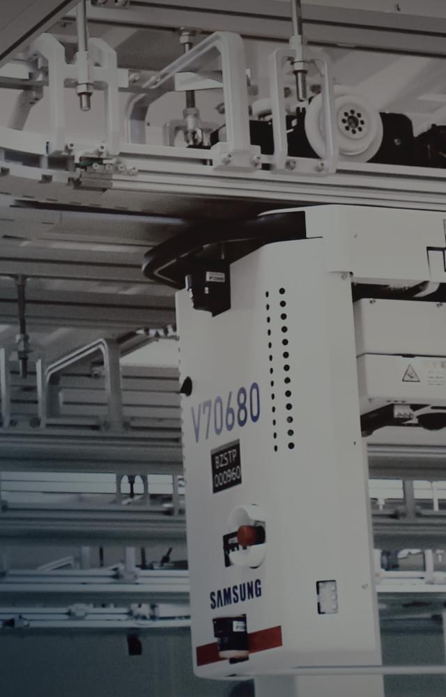
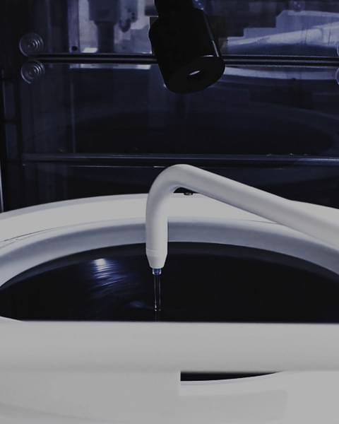
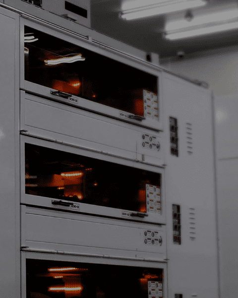
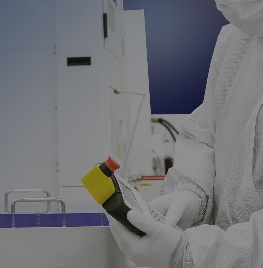
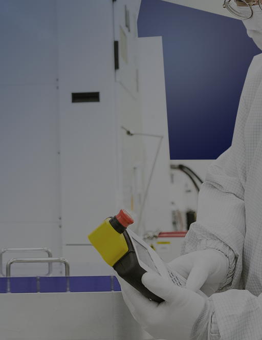
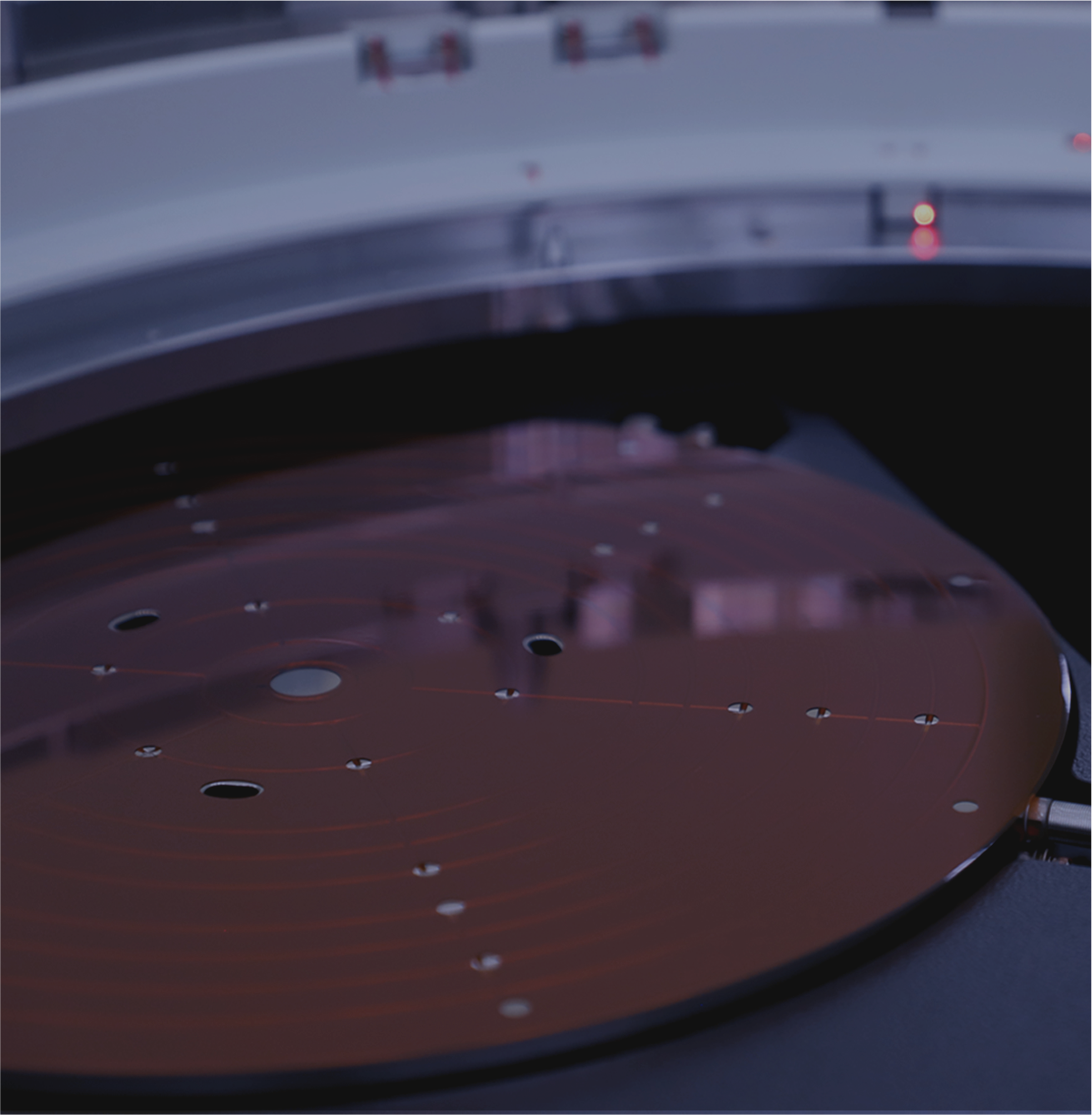
Regarding the semiconductor sector, we are producing equipment
for cleaning , photo track, and etcher.

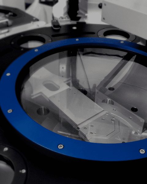
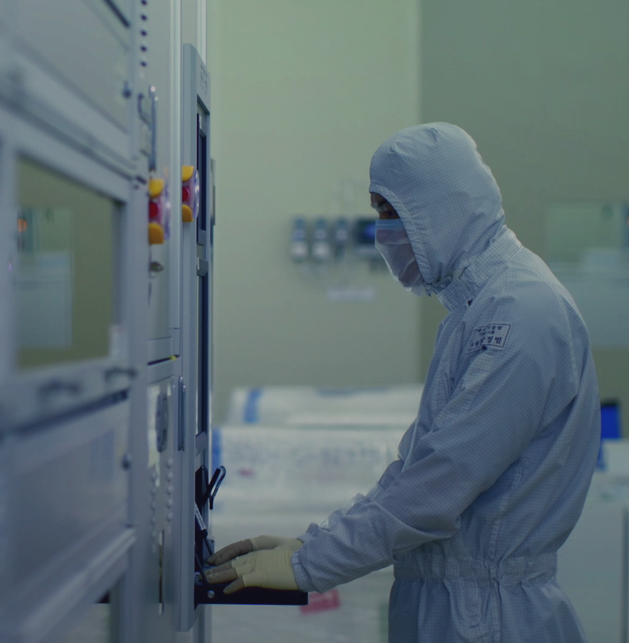
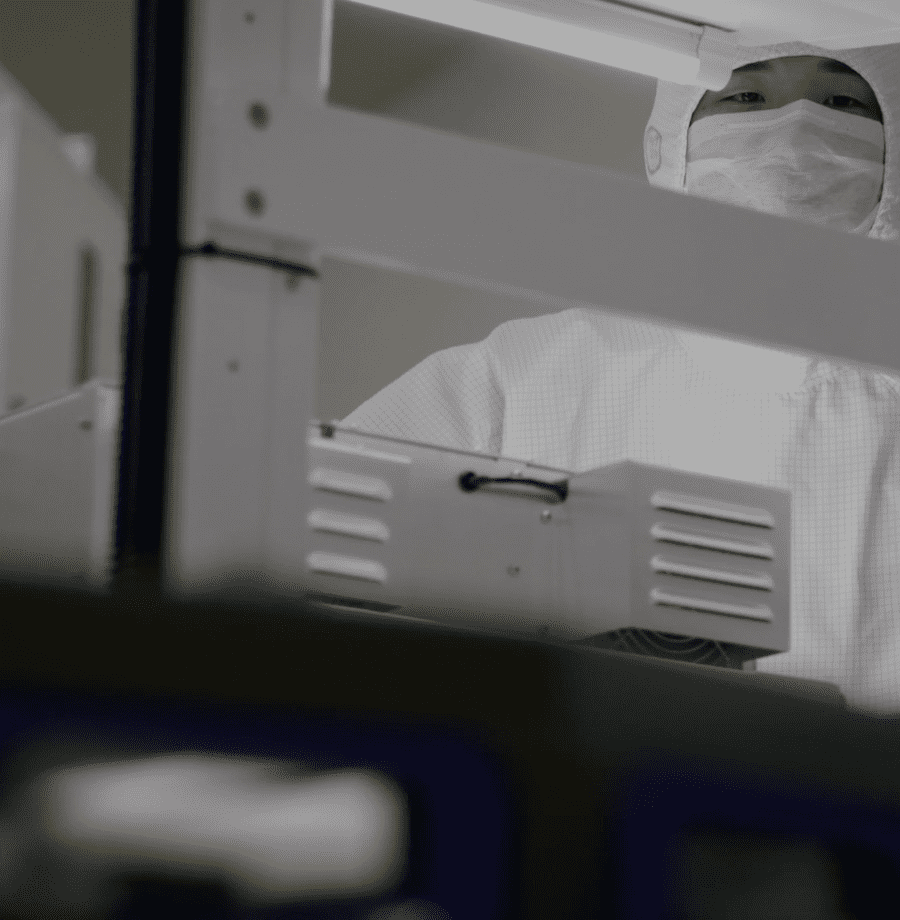
The semiconductor/display
equipment business is
a
high-tech industry that
requires highly-advanced
technical
skills and rich
expertise.
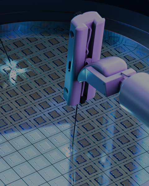
The semiconductor/display
equipment business is
a
high-tech industry that
requires highly-advanced
technical
skills and rich
expertise.
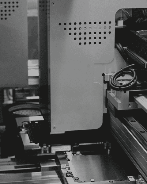
The semiconductor/display
equipment business is
a
high-tech industry that
requires highly-advanced
technical
skills and rich
expertise.
The semiconductor/display
equipment business is
a
high-tech industry that
requires highly-advanced
technical
skills and rich
expertise.
The semiconductor/display
equipment business is
a
high-tech industry that
requires highly-advanced
technical
skills and rich
expertise.
SEMES creates new opportunities with differentiated technology.